| |
 |
| |
|
 |
 |
|
01/2017 |
|
Düsseldorf, 03.01.2017
|
| |
|
| |
|
|
Dear Photonics21 member
|
In this newsletter we want to inform you about the newly elected president and the new members of the Photonics Board of Stakeholders.
Please remember to already mark the calendar for the Photonics Public Private Partnership Annual Meeting 2017. Registration will open soon.
We released news stories about the Photonics PPP projects MIREGAS and LUMENTILE. Read through the stories and get information on the device which can detect various gases to prevent global warming. Get an idea what newly created ceramic tiles can do for smart homes.
Apply for our eights Student Innovation Award! You want to become a Sponsor of the Award? Great! Contact us and we will provide you the details.
If you would like to inform the Photonics21 membership on any photonics activities or events within your national or regional photonics community or provide us your feedback to the Photonics21 newsletter you can send it to SECRETARIAT@PHOTONICS21.ORG.
Best regards
Secretariat Photonics21
SECRETARIAT@PHOTONICS21.ORG
www.photonics21.org
https://twitter.com/Photonics21
https://linkedin.com/company/photonics21
|
|
|
|
|
 Congratulations to the newly elected Photonics21 president Aldo Kamper, CEO Osram Opto Semiconductors GmbH.
Aldo was elected by the Board of Stakeholders on November 22nd.
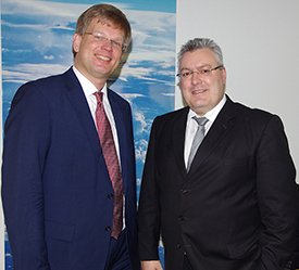
Right: Dr. Michael Mertin, left: Aldo Kamper
After Dr. Michael Mertin announced to step down from this highly valued position Photonics21 is happy to have found someone willing to take the lead on the challenges the Community is facing in the coming years.
|
|
|
|
Firstly a big thank you to all representatives who casted their vote on our BoS election 2016. We, again, had a very good voting participation of 75%.
Congratulations to our new Board of Stakeholder members:
| ADIGE S.P.A. |
Sbetti
|
Maurizio
|
|
asphericon GmbH
|
Kiontke
|
Sven
|
|
CEA LETI
|
Fulbert
|
Laurent
|
Centro de Estudios e Investigaciones Técnicas
(Ceit-IK4) |
Olaizola
|
Santiago Miguel
|
|
Horiba
|
Jacquemin
|
Sylvain
|
Institute of Photonics and Electronics Academy
of Sciences of the Czech Republic |
Homola
|
Jiri
|
|
KARL STORZ GmbH & Co. KG
|
Leonhard
|
Martin
|
|
LASEA SA
|
Ramos de Campos
|
Jose Antonio
|
|
Leica Microsystems Group
|
Burke
|
Julian
|
Max-Planck-Gesellschaft zur Förderung der
Wissenschaften e.V. |
Marquardt
|
Christoph
|
|
PhoeniX B.V.
|
Korthorst
|
Twan
|
|
Photonics Austria
|
Trog
|
Ulrich
|
|
Politecnico di Milano
|
De Silvestri
|
Sandro
|
|
SWANSEA UNIVERSITY
|
Taccheo
|
Stefano
|
|
Universidad Carlos III de Madrid
|
Guillermo
|
Carpintero
|
|
Zumtobel Group
|
Seyringer
|
Heinz |
|
|
|
|
The next Photonics Public Private Partnership Annual Meeting has been scheduled on the 28th and 29th March 2017. The event will be held in Brussels. We kindly invite you to already mark the date in your calendar. Any further details will be communicated and published on the Photonics21 website www.photonics21.org within the next weeks.
|
|
|
|
 Using the latest photonics technology a group of European scientists are developing a multi-gas detector that can spot dozens of harmful emissions with a single sensor in milliseconds, delivering a breakthrough for the prevention of climate change.
The Intergovernmental Panel on Climate Change (IPCC) estimates that concentrations of Methane (CH4) in the atmosphere are roughly two and a half times those of pre-industrial times. The primary component of natural gas, Methane is over 20 times more effective at trapping heat than carbon dioxide and can remain in the atmosphere for more than a decade.
With natural gas and petroleum systems being the largest source of CH4 emissions from industry, and with the USA pledging a 40-45% reduction in methane emissions from 2012 levels by 2025, it has never been more important to have effective monitoring equipment.
Exploiting new photonics technology, the H2020 project MIREGAS (‘Mid-IR source for Gas Sensing’) has come up with their solution: a novel, low cost sensor that has the potential to be programmed to detect an unlimited number of gases.
The first of its kind, MIREGAS aims to deliver a single, multi-band gas sensor that can be easily deployed in strategic points of methane emissions, such as on oil rigs or in industrial areas, and monitor dozens of Greenhouse gasses all at once.
While current technology can take up to 10 seconds to produce a positive ID, the device can detect dozens of harmful emissions in milliseconds, making it several thousand times faster state of the art gas sensors, and, effectively a real-time instrument.
The size of a mobile phone, the gadget can pick out poisonous gases from a mixture of emissions, including methane, ethane, butane, propane, CO2, carbon monoxide, hydrogen sulphide and benzene, all from one compact filter.
Combining the principles seen in fibre optic communications, the MIREGAS gadget exploits multiplexing-to-demultiplexing filters, modulating and wavelength tuning, with Mid-IR spectroscopic sensing technologies, a process never seen before.
Professor Pentti Karioja from the VTT Technical Research Centre of Finland Ltd, explains:
“Because the MIREGAS device is adjustable, it is possible to use only one light source instead of several lasers. This means that we can make multiple readings and monitor several harmful gases simultaneously through one sensor.”
While Mid IR spectroscopic equipment exists, current sensors are based on the use of filters, spectrometers or tuneable lasers, meaning a several lasers would be needed for corresponding gases.
“The possibility to tailor a spectral response to match any wanted set of absorption lines with any desired bandwidth is a major advantage of our filtering approach when compared to the single narrow line of a tuneable laser”, said Karioja.
Initially the MIREGAS device is expected to be deployed in several industrial fields such as building ventilation, process control and safety, gas leakage monitoring, personal, pipeline and explosion safety. However the capabilities for observing dangerous greenhouse gasses in our atmosphere will provide practical tools for tackling climate change.
Pawel Kluczynski of Airoptic, a key partner in the MIREGAS consortium, says:
"Excessive methane emissions are dangerous, and can have a considerably greater warming effect than carbon dioxide. The widespread application of methane emission detection, as well as all of the hydrocarbons from C1 to C5 is a key area for the MIREGAS technology.”
“Not only are our measuring costs ten times cheaper than methods used today but our spectral resolution is 10 times better compared to conventional MOEMS filters used currently in gas sensors. It offers 24/7 protection, there is no need for recalibration and you don’t need a Ph.D to operate it.”
At the foreseen manufacturing cost of below €300 per unit, the proposed approach is extremely competitive against conventional gas sensors which can cost in excess of €75,000. “These devices currently in the market are either expensive complicated and heavy instruments, or the applied measurement principles are inadequate in terms of stability and selectivity” said Kluczynski
Coordinated in Finland by VTT, the MIREGAS project has received a grant of €3,588,262 from H2020 via the Photonics Public Private Partnership. MIREGAS is comprised of a consortium of members from Finland, Poland and Norway, including Tampere University of Technology, Vaisala OYJ, the Instytut Technologii Materialow Elektronicznych, Airoptic Spolka z Ograniczona Odpowiedzialnoscia, Vigo System S.A. and Gassecure AS
|
|
|
|
 Redecorating your living room could be as easy as pressing a button thanks to European scientists who have created a new ceramic tile that can change colour, pattern, or play videos with one tap of your finger, radically changing the way we interact with buildings or public spaces, and taking us a step closer to instant camouflage.
Ever wanted to make your living room look like the inside of an art gallery, a Stone Age hut or Buckingham Palace? Have you wanted to redecorate your bedroom every day of the week, or watch films on your ceiling? Now you can, thanks to this digital ceramic panel created by Italian scientists.
Using pioneering photonics technology, The 'Luminous Electronic Tile', or LUMENTILE, project mixes the simplicity of a plain ceramic tile with the complexity of today's sophisticated touch screen technology, creating a light source and unparalleled interaction. All it takes is one tap to change the colour, look or mood of any room in your house.
This is the first time anyone has tried to embed electronics into ceramics or glass for a large-scale application. With the ability to play videos or display images, the tiles allow the user to turn their walls into a large ‘cinema’ screen, where each unit acts as a set of pixels of the overall display.
A combination of ceramic, glass and organic electronics, the luminous tile includes structural materials, solid-state light sources and electronic chips and can be controlled with a central computer, a smart phone or tablet.Project coordinator, Professor Guido Giuliani of the University of Pavia explains:
“This is not just a digital panel to replace an animated poster like you see on the Underground network, but a whole new way of life. You are instantly in control of your own environment: if you don’t like your bathroom in blue, now you can change it to green with one tap. If you like flowery wallpaper, ducks or Christmas trees, that’s up to you.”
Each measuring the size of a standard, rectangular A3 piece of paper with their own internal power source, the tiles can be tailored entirely to the customer’s needs: completely or partially covering the walls of a room, a floor, ceiling, or perhaps total submersion. So long as the pieces tessellate, any shapes will be possible such as hexagonal or triangular ceramic tiles.
The tiles, which can be switched off so that a basic silver, black or white colour can be a default setting, are equipped with an on board micro-controller, and operate on a lexical network invisible to the user. The surface of each tile has uniform and efficient illumination, achieved by LUMENTILE’s smart light management system, a new approach based on a light guiding slab and spatially selective light extraction.
Exterior ‘Chameleonic Skin’
With its durable nature, the luminous ceramic tile holds boundless possibilities: placing it on the outside of a building creates the obvious potential for advertising or changing the colour or appearance. However the tiles can be flat or curved to fit around columns or uneven contours.
Military vehicles, for example, fitted with this external ‘skin’ crossing a variety of terrains, such as woodland, desert or water would be capable of unlimited camouflage at the flick of a switch.
“It may sound like the stuff of James Bond but external tiles would createa ‘chameleonic skin’, or instant camouflage. Although we are a long way off this yet,thiswould allow a car or building to blend completely into its surroundings, and hence ‘disappear’,” Giuliani enthused.
Smart Floors
With the ability to configure the tiles to become ‘smart floor panels’ that recognise when an elderly user is no longer standing or has perhaps fallen, in security situations where a floor will be sensitive to intruders, or in shopping centres where a ‘dynamic path’ can be created to direct shoppers to a particular store, the LUMENTILE product is more than just a light source.
Earlier this year LUMENTILE received a grant of € 2,470,113.75 from Horizon 2020 via the Photonics Public Private Partnership. Hoping to be available to users in two years the LUMENTILE project aims at mass production by the end of 2020.
Coordinated in Italy by UNIVERSITA DEGLI STUDI DI PAVIA, LUMENTILE is comprised of a number of partners from Finland, Italy, Switzerland, Spain, including TEKNOLOGIAN TUTKIMUSKESKUS VTT (Finland), ECLEXYS SAGL (Switzerland), JULIGHT SRL, KERAPLAN SRL (Italy), STUDIO ITINERANTE ARQUITECTURA SL, KNOWLEDGE INNOVATION MARKET S.L. (Spain).
|
|
|
|
For the eights time the ETP Photonics21 announces the Photonics21 Student Innovation Award. The prize will be handed over in the frame of the Photonics21 Annual Meeting on the 28th and 29th of March 2017.
Background:
The Research, Education and Training work group of the Photonics21 Technology Platform has established a prize for students in the field of photonics in order to promote research in photonics especially related to R&D with industrial impact.
Any person under 35 and active in the field of optics and photonics may apply for the Photonics21 Student Innovation Award. The award consists of a certificate, a trophy as well as a cash prize of € 5,000.
Applicants must submit the following documents:
- The completed application form,
- One letter of support (by a supervisor or mentor),
- A short (2 page) biography/CV
- A list of peer reviewed publications
- A description of the innovative R&D work (not exceeding 4 pages of A4, 12 point text), making clear the nature of innovation potential impact to industry
The application deadline for participating in the Photonics21 Student Innovation Award 2017 is the 20th of January 2017.
Applications can be sent via e-mail to education@photonics21.org.
Sponsoring
If you would like to sponsor either the Photonics21 Annual Meeting or the Student Innovation Award, please download the presentation for more information or contact the Photonics21 Secretariat at secretariat@photonics21.org
|
|
|
|
 Join – PIC International Conference, 7-8 March 2017, Brussels, Belgium Join – PIC International Conference, 7-8 March 2017, Brussels, BelgiumSales of PICs are soaring, with their deployment helping to boost the capacity of networks and data centres. To aid this industry, we are strengthening the relationships between the makers and the users of these integrated circuits by organising the 2nd PIC International, a global conference dedicated to this industry.
In 2017, the conference grows to a new auditorium to welcome more industry leaders and rising stars driving the next generation of photonic integrated circuits. Speakers confirmed to date include IBM, Infinera, Seagate, Luxtera, imec, VTT Research, the European Space Agency, and many more, view the agenda to date here - view abstracts.
Key themes include a deep dive into PIC platforms, manufacturing solutions, device deployment in data centres, telecoms and a full update on activity in emerging markets such as life sciences. Full details on all of the conference tracks together with advance speaker profiles are now available to view on www.picinternational.net
Early bird registration
The 2nd PIC International event brings together the best in class of the integrated photonics industry. Book your place before 30th November 2016 and take advantage of our early bird discounted rate, saving €100.
Be a part of it - speaking and sponsorship/exhibiting opportunities available
Sponsorship information: http://mediapack.picinternational.net/
The sponsor packages provide companies with an influential industry platform to educate and penetrate the world wide integrated photonics industry by a multitude of marketing methods over a 6 month period.
Tel: +44 (0)2476 718970
Website: www.picinternational.net
Email: info@picinternational.net
|
|
|
|
 Join – German Biosensor Symposium 20-23 March 2017, Potsdam, Germany Join – German Biosensor Symposium 20-23 March 2017, Potsdam, GermanyThe German Biosensor Symposium is a bi-annual event, first held 1999 in Munich. After 2001 in Potsdam it was held in several locations, the hot spots of Biosensor research in Germany. In 2017, it will be extended to the first European Biosensor Symposium. The Symposium not only draws attention to young scientists to make their first steps in their academic career but also attract seniors and companies to learn about the most recent trends of biosensor research and technology, but also to see who the drivers of the development are.
When: March 20-23, 2017
Where: University of Potsdam, Campus Griebnitzsee, 14483 Potsdam, Germany
Abstract submission + registration open September 1, 2016.
All important information (Topics, Deadlines etc.) can be found under: http://www.ebs2017.com/
|
|
|
|
|
| |
|
|
|